Do you like DIY and default footprints in PCB CAD programs are not satisfying? Create your own. But what are the dimensions and placement positions? Datasheets and some calculations can help a lot.
Eagle has a very decent default library with usable footprints. But I switched to KiCad and its default library sucks. Fortunately footprint creation is extremely easy there. So I decided to make my own from scratch (note: I like the KiCad’s way of independent schematic symbols and footprints very much). Base units will be millimeters with exceptions where inches will give an exact dimension/distance. All X/Y coordinates will be relative to the midpoint of the footprint or pad. Lets start with some SMD stuff.
SMD
SO-8/SOIC-8 narrow
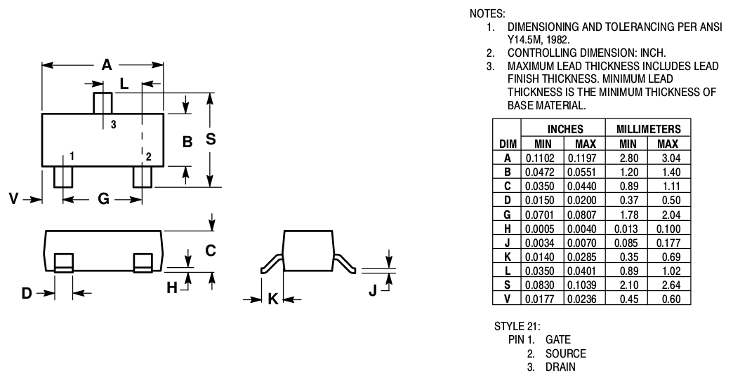
This package is probably the most common package for 8-leaded packages like 555 timer and low-to-mid power transistors. IRF7413 transistor datasheet is a great sample with a footprint recommendation:
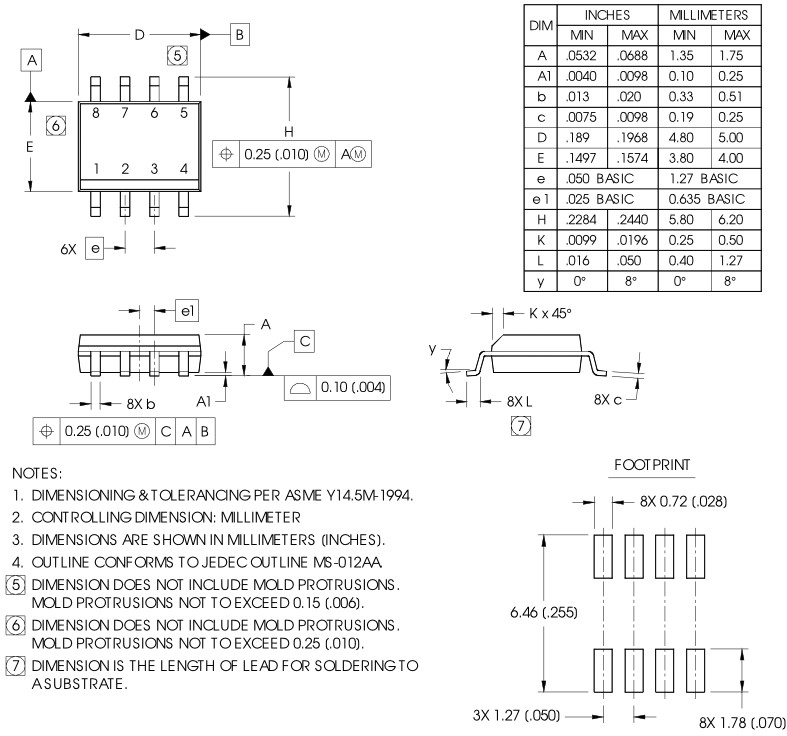
Depicted footprint (bottom right corner) is probably specified for machine pick’n’place and reflow soldering. I solder by hand so I need some minor corrections. The main task is to cover all dimension ranges and leave some room for hand placement and soldering.
You must definitely keep the pads midpoints spacing 0.05″ (1.27 mm) – X coordinates of the pads will be {-0.075″, -0.025″, 0.025″, 0.75″}. The width of 0.72 mm is not bad so keep it. Make the pads longer. Start with the edge most distant from the center ED.
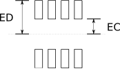
You need to take the maximum value of H plus some space for soldering. My choice is 0.5 mm which proved to be sufficient. The formula for the distant edge is then:
ED = max(H) / 2 + 0.5
In this case it is ED = 6.2 / 2 + 0.5 = 3.6 mm. Now the closest edge EC – you need the minimum value of H and subtract maximum length of the “sitting” part of the lead and also minus some space. This space is not very important because it is almost out of the soldering area but it can help with alignment if you are unlucky and you will get the package with the smallest tolerated dimensions. 0.2 mm should be enough. Formula:
EC = min(H) / 2 – max(L) – 0.2
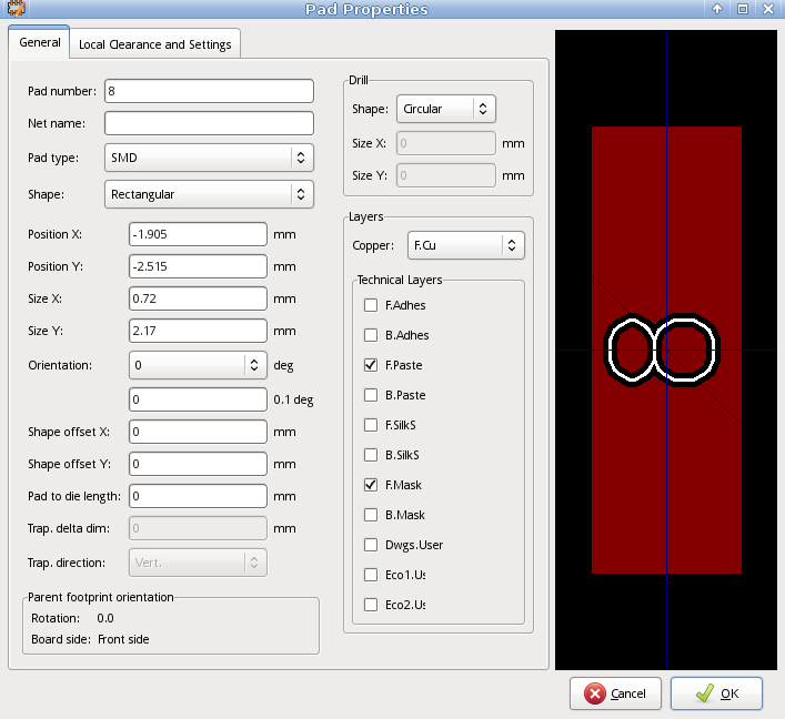
In this case EC = 5.8 / 2 – 1.27 – 0.2 = 1.43 mm. Pad height is ED – EC = 2.17 mm. And the pad center Y = (ED + EC) / 2 = 2.515 mm. Following screenshot is from KiCad pad editor:
SOT23-3
This package type is used often for low power transistors. Lets see the datasheet of ON Semiconductor 2N7002:
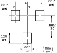
Datasheet contains minimum recommended footprint. This is useless. The minimum width here is 0.8 mm but since the leg width (max(D) = 0.5 mm) is the same as with IRF7413 it can be 0.72 mm as well. I miss the leg “sitting” part length here. Another datasheet is neccessary – BSS84:
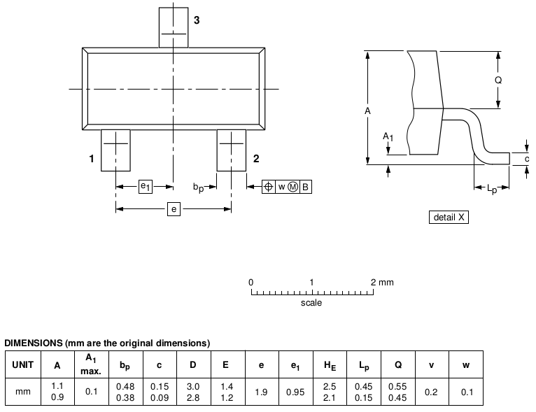
Now we can calculate. ED = 2.64 / 2 + 0.5 = 1.82 mm, EC = 2.1 / 2 – 0.45 – 0.2 = 0.4 mm. The rest is easy.
SMA
Power diodes in SMA(B, C) packages do not have leads like the small outline packages. They are more similar to SMD resistors or capacitors. Their leads are bent below the package. You need more hand soldering space. SSA33L:
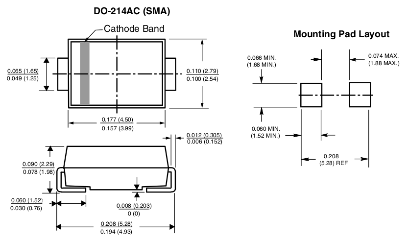
Mounting pad layout is suited for reflow soldering. Be assured that you will have huge problems soldering that with a soldering iron. Prolong the pads and you are fine. ED = 5.28 / 2 + 1.2 = 3.64 mm, EC = 4.93 / 2 – 1.52 – 0.2 = 0.75 mm.
THT
Through hole technology/packages with leads are much easier. In most cases. You now the exact leads distance and thickness.
Capacitor
E.g. radial electrolytic capacitor, 1000 uF, 10 V: lead thickness 0.6 mm, distance 5 mm (different manufacturer might have different sizes for the capacitor rating, always look into the datasheet). You have to choose right drill size and pad diameter. There are inaccuracies in the drill bit thickness and drill positioning especially if you are doing it at home, you will never hit the spot right 🙂 For 0.6 mm you can use 0.8 mm drill bit. How about the pad diameter? Two variables come into the play – easy solderability/inaccuracy resilience (the bigger pad the better) and space saving (the smaller the better). 2 mm in diameter should be enough.
Pin header
Here comes the fun. Pins are squared with the side length of 0.64 mm. So the wrapping circle diameter is ~0.9 mm (simple Pythagoras). Drill size should be at least 1.1 mm (0.9 mm lead diameter + 0.2 mm spare) so you will not tear off the plating. Pads centers distances are 0.1 inch. If you don’t need to place a trace between the pins then you can set the size quite large. But this is a waste of space. Count with me: I need a 12 mils trace with 11 mils clearance – 34 mils/0.034 inch space between the pads: pad size/diameter = 0.1 – 0.034 = 0.066 inch.
Little observation for KiCad zones fill – for the pin pad size mentioned above the zones will not fill areas between the pads (zone minimum width 12 mil, clearance 11 mil) due to the filling mechanism. Shrinking the pad size to 0.063 inch works well.
No Comments
No comments yet.
RSS feed for comments on this post.
Sorry, the comment form is closed at this time.